Timing
The time when display refresh frame could be measured directly. A Marker, usually small square at corner of viewport on the topmost layer, could flip between two colors, e.g. black and white, in different frames. A photodiode can be placed on the Marker converting light intensity to electrical signal. By recording and analyzing the signal, the light intensity change time can be extracted and that would be the exact frame change time.
Because the Marker is flipping between two colors, it would be natural to convert the photodiode analog signal to digital signal and it can be done in real-time by a Photodiode Logic Board.
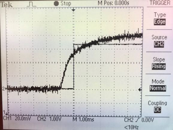
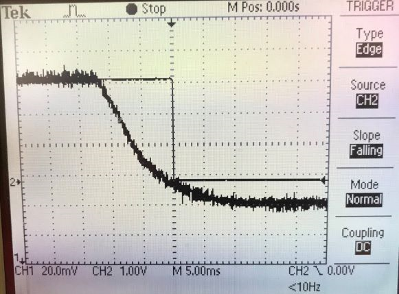
The asymmetric display response time between Black->White, i.e. rising and White->Black, i.e. falling could introduce different lags when photodiode analog signal being threshold and converted to digital signal. To get the exact frame change time, these two lags should be measured and saved for the specifically configurated display and used later to correct the digital signal flip time.


Usually, any experimental event that need to notify external device will send signal through at least two channels. The first channel(Sync) often goes through digital GPIO(<0.1ms latency), marking the time event issued. The second channel(Measure) is by photodiode detecting exact time of event happening on display. Usually, signals in these two channels are the same, providing extra robustness, in case of signal corruption.
The Experica has a internal timeline that are used to manage all experiment logic. The event time on this timeline(Command) could be converted to external device Sync time by a time zero delay and timer drift speed between Command and the device. These parameters and display latency could be calculated based on data, and used to correct any corrupted data. They will be evaluated automatically during the DataExport.
Here shows condition duration from photodiode real-time digital convertion, corrected by above asymmetric display response time.
.svg)
.svg)